Measuring the Fmax of Integrated Circuits
02 Nov 2023
A great deal of good, quick, cost-effective EMC design depends upon the highest frequency at which ICs can cause EMC problems, which is constantly increasing due to developments in semiconductor manufacturing [1].
As well as needing to be taken into account in new projects, these developments can cause serious EMC problems for products that are manufactured for more than 2 years or so.
We might not care, if not for the fact that – in real life – products that don’t comply with the relevant standards listed under the EMC Directive tend to have increased warranty claims and worse customer experiences [2], perhaps leading to reduced market share.
When a new IC manufacturing process is qualified, most ICs ‘migrate’ to it, to achieve higher yields to increase the profitability of their manufacturers. However, these important changes are only indicated by the batch numbers of the ICs, and – although the ‘new-process’ ICs may need improvements to a product’s EMC design – we can’t get any to test until about 6 months before the older versions cease being made, a timescale that has cost some companies tens of thousands of Pounds, even threatened them with bankruptcy.
My training courses [3] [4] often rely on knowing the highest frequency at which ICs can cause EMC problems, which I call Fmax and section 1.18 in [5] has a detailed discussion of this concept. But how can we discover this important IC information?
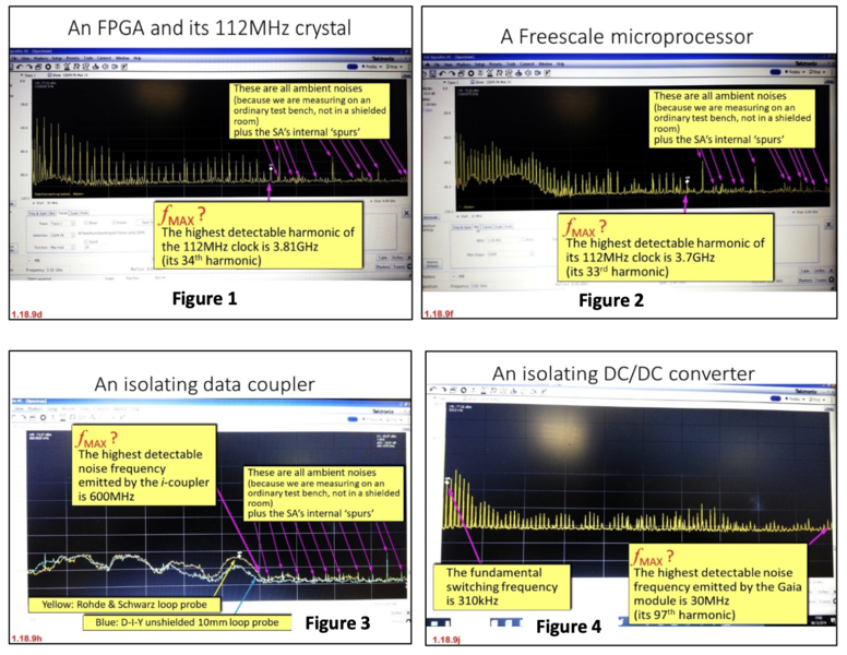
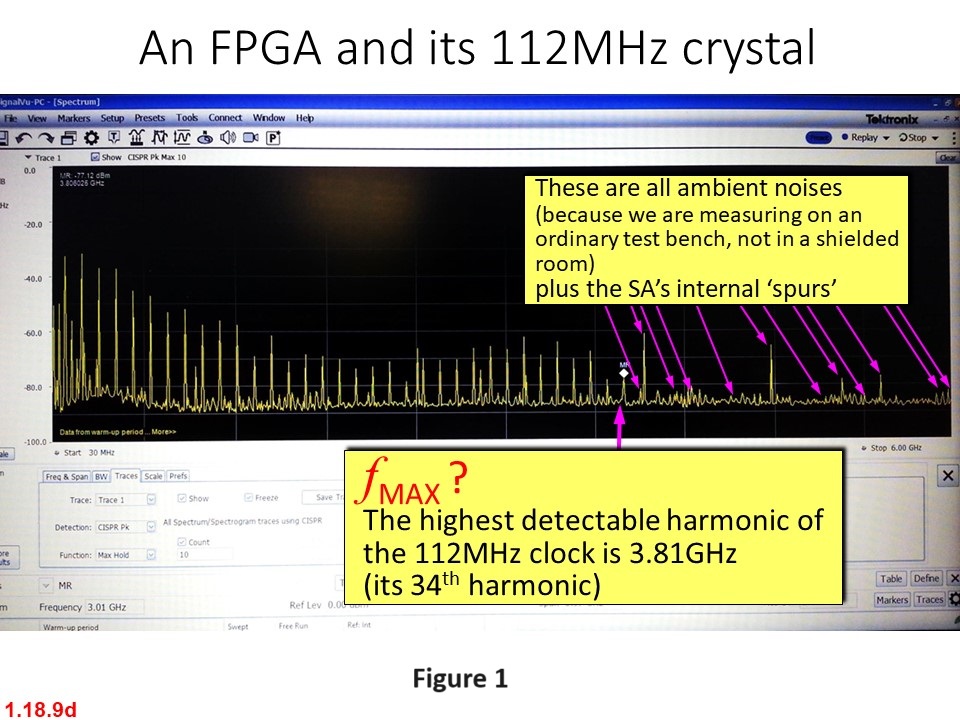
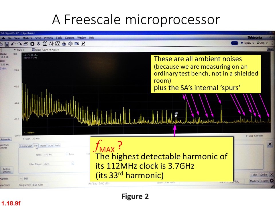
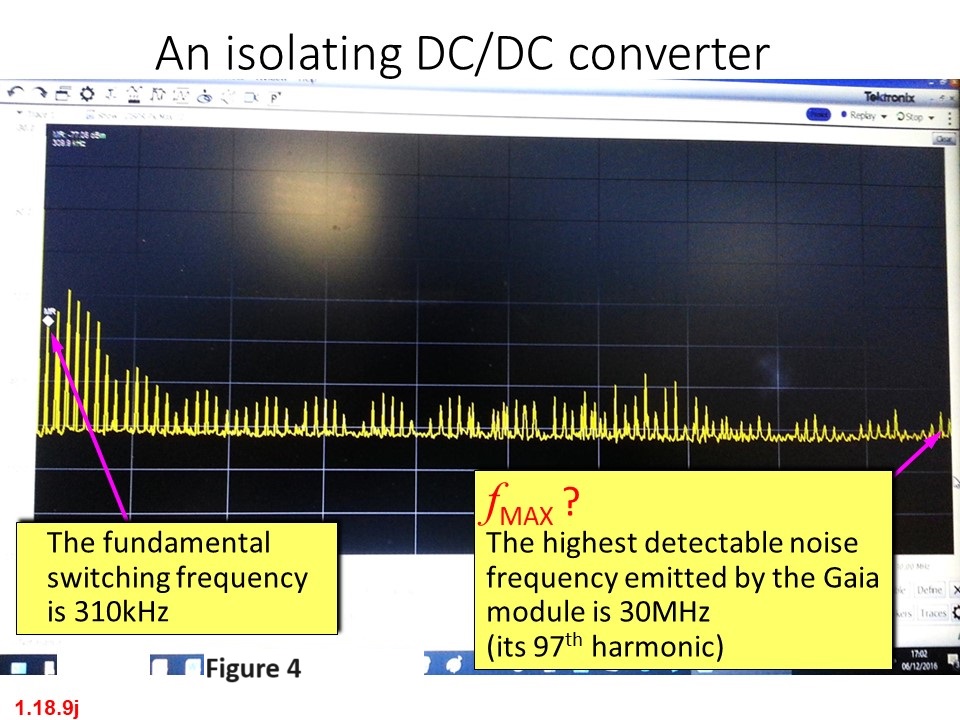
Figures 1 - 4 show quick, D-I Y, measurement results of Fmax for three ICs and one module.
We would prefer device manufacturers to apply at least one EMC test method for radiated, and one for conducted, from both the IEC 61967 series (emissions) and the IEC 62132 series (immunity) listed below, and publish their results with the rest of their IC data.
However, if this data isn’t available, most of these tests are relatively easy to do yourself – using low-cost EMC test gear and D-I-Y probes as described in [6].
IEC 61967: Integrated circuits – Measurement of electromagnetic emissions
IEC 61967-1:2018, General conditions and definitions,
inc. test method comparison tables (Annex A),
and the design of a standardised test board (Annex D)
IEC TR 61967-1-1:2015, Near-field Scan Data Exchange Format
Radiated emissions
IEC 61967-2:2005, TEM Cell and Wideband TEM Cell method
IEC TS 61967-3:2014, Surface Scan method
IEC 61967-8:2023, IC Stripline method
Conducted emissions
IEC 61967-4:2021, 1 ohm/150 ohm Direct Coupling method
IEC TR 61967-4-1:2005, Application guidance to IEC 61967-4
IEC 61967-5:2003, Workbench Faraday Cage method
IEC 61967-6:2002+A1:2008, Magnetic Probe method
IEC 62132: Integrated circuits – Measurement of electromagnetic immunity
IEC 62132-1:2015 General conditions and definitions,
including test method comparison tables,
and the design of a standardised test board
Radiated immunity
IEC 62132-2:2010 TEM cell and wideband TEM cell method
IEC 62132-8:2012 IC stripline method
IEC TS 62132-9:2014 Surface scan method
Conducted immunity
IEC 62132-4:2006 Direct RF power injection method
IEC 62132-5:2005 Workbench Faraday cage method
Note: ‘close field’ and ‘near field’ are not the same, but are often used interchangeably.
The Surface Scan method in IEC TS 61967-3 is similar to the one described in “Cost Effective Uses of Close Field Probing” [4]: with the spectrum analyser set to ‘Max Hold’, simply move a close-field RF probe around on the top of the functioning device to maximise the displayed spectrum measurement until it doesn’t change anymore.
This can be done when the device is mounted on a demo board, or on a prototype PCB (as I did for Figures 1-4 above), when it is functioning as required, or in the worst-case(s) that might be required.
The official IEC method is much better controlled and produces a lot of useful data, not least for improving an IC’s internal design.
But – when all we need to know is an IC’s Fmax – my much quicker approach, which can be done in most situations, is all that is really needed.
You may also be interested in:
IEC 62014-3:2002, Models of Integrated Circuits for EMI Behavioural Simulation
– and in:
Basic Concepts in EMC for ICs, Springer, 1985,
https://link.springer.com/chapter/10.1007/0-387-26601-1_1
References:
[1] https://www.emcstandards.co.uk/moores-law-die-shrinks-and-cost-effective-emc
[2] https://www.emcstandards.co.uk/we-don-t-do-emc-for-the-sake-of-the-ce-markin
[3] https://www.emcstandards.co.uk/emcacademy
[4] https://emcstandards-shop.fedevel.education/index.html
[5] https://www.emcstandards.co.uk/the-physical-basis-of-si-pi-and-emc
[6] https://www.emcstandards.co.uk/cost-effective-uses-of-close-field-probing1
Get more from EMC Standards
EMC Standards is a world-leading resource for all things EMC and EMI related. Our website is packed full of both free and paid-for content, including:
- Online quiz
- Webinars
- Training quiz
- And much more!

Electromagnetic Engineering (EMgineering) is the basis for proven good design practices for signal integrity (SI), power integrity (PI), and the control of EMI emissions and immunity (EMC).
Our aim is to help people learn how to more quickly and cost-effectively design and manufacture electronic equipment (products, systems, installations, etc.) to meet functional (i.e. SI/PI) specifications and conform to EMC standards, directives and other requirements.
Such equipment should benefit from reduced warranty costs and financial risks, whilst improving uptime, competitiveness and profitability.
We also cover basic good electrical safety engineering; and the Risk Management of Electromagnetic Disturbances / EMI, whether for Functional Safety or other types of risk.
Join EMC standards TODAY!