Ground / power bounce cause noise emissions from all IC pins
14 Feb 2020
Ground / power bounce cause noise emissions from all IC pins
Ground and power bounce are often ignored as sources of CM noise emitted from all integrated circuit (IC) pins, even if they are static inputs or outputs, digital or analogue, and even sometimes emitted as radiated noise directly from the body of the IC (especially when its physical structure resonates).
CMOS ICs use ‘totem-pole’ logic switching gates that momentarily short their Vdd and Vss power rails together every time they change state, see the figure below, and www.emcstandards.co.uk/part-5a-decoupling. A CMOS logic gate can be thought of as effectively being a ‘make-before-break’ switching element.
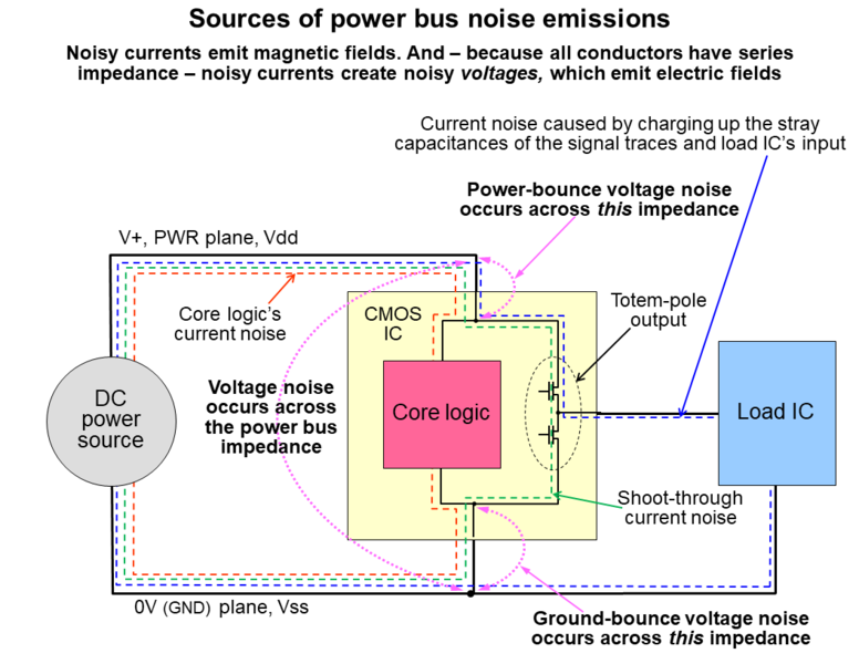
There is always some series resistance and inductance in the connection of an IC’s Vdd and Vss pins to the corresponding power planes on their printed circuit board (PCB). On a modern ball grid array (BGA) IC there are usually many dozens of Vdd and Vss pins, connected in parallel, to try to minimize this series resistance and inductance, but it cannot be totally eliminated.
Whenever the CMOS totem-pole logic gate switches and momentarily shorts out the power rails, a large transient current flows in both the IC’s and the PCB’s power distribution system, often called a ‘power transient current’ or ‘shoot-through current’.
As this very brief but intense pulse of current flows through the series impedance between the IC’s Vdd and Vss pins and their corresponding power planes on the PCB, it creates transient voltages. The transient voltages arising between a logic low level and the Vss (or 0V) plane on the PCB are called Ground Bounce, while the transient voltages arising between a logic high level and the Vdd (or PWR) plane on the PCB are called Power Bounce.
Ground and Power bounce are thus noises on the logic output signals, and if they are large enough with respect to the noise threshold they can cause false-triggering of subsequent logic gates.
Another issue with Ground and Power bounce, and the subject of this brief article, is that CMOS devices containing digital processing or memory are constantly being clocked, so even if the outputs are not changing state, many thousands – even millions – of internal logic gates are changing state every second, each one shorting the power rails out every time. So there is always ground and power bounce noise being generated between such an IC’s power distribution network and its PCB’s power distribution network.
The entire IC is constantly ‘buzzing’ with ‘ground/power bounce’ voltage noise with respect to the PCB’s Vss power plane, which is usually the 0V (or GND) plane – the board’s RF Reference plane. This means that all of the IC’s input and output pins are also buzzing with ‘ground/power bounce’ voltage noises with respect to the board’s RF Reference, whether the I/O data is changing or not.
This ground/power bounce noise is common mode (CM) noise, because it appears on all of the IC’s pins, including inputs, power pins, programming pins, voltage reference pins, etc. It extends right up to the highest harmonic frequency generated by the IC’s core logic, which uses the smallest transistors and so switches much faster than the (relatively) large and slow I/O transistors, creating much higher-frequency harmonics than the output transistors do when they switch.
We often notice that emissions plots show even-order harmonics of a PCB’s clock frequency (2nd, 4th, 6th, etc.), even though the clock is a good squarewave. Pure squarewaves only contain odd-order harmonics (3rd, 5th, 7th, etc.) , so where are these even-order harmonics coming from?
The effect of shorting the power rails out on each logic gate switching edge, is that the power transient currents run at double the clock rate. So for example a clock with a fundamental frequency of 100MHz creates odd-order harmonics (e.g. at 300MHz, 500MHz, 700MHz, etc.)and creates ground/power bounce CM noise at the fundamental frequency of 200MHz, with both even and odd-order harmonics (because it is not a square wave) at 400MHz, 600MHz, 800MHz, etc. – all of which are even-order harmonics of the original 100MHz clock.
So when we measure excessive emissions from our products at even-order multiples of a clock’s frequency, we should suspect ground/power bounce noise in CMOS ICs as being the cause.
Get more from EMC Standards
EMC Standards is a world-leading resource for all things EMC and EMI related. Our website is packed full of both free and paid-for content, including:
- Online quiz
- Webinars
- Training quiz
- And much more!

Electromagnetic Engineering (EMgineering) is the basis for proven good design practices for signal integrity (SI), power integrity (PI), and the control of EMI emissions and immunity (EMC).
Our aim is to help people learn how to more quickly and cost-effectively design and manufacture electronic equipment (products, systems, installations, etc.) to meet functional (i.e. SI/PI) specifications and conform to EMC standards, directives and other requirements.
Such equipment should benefit from reduced warranty costs and financial risks, whilst improving uptime, competitiveness and profitability.
We also cover basic good electrical safety engineering; and the Risk Management of Electromagnetic Disturbances / EMI, whether for Functional Safety or other types of risk.
Join EMC standards TODAY!